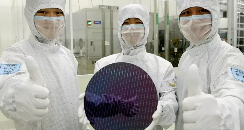
According to a report from TheElec and Samsung’s presentation at this year’s Very Large Scale Integration (VLSI) Symposium, the semiconductor manufacturer used new backside power delivery network (BS-PDN) approaches to successfully reduce the required wafer area by 14.8% when compared to traditional front side power delivery networks (PDNs).
Read Entire Article

